Expertise and decades of experience: Etching technology at Possehl Electronics

Produced etched parts p.a.
~40000000 pcs.Materials
- Copper alloys with a thickness of 0.102 mm (4 mil) to 0.508 mm (20 mil)
- The most important copper alloys are C19400, C70250, EFTEC-64T and C15150 with different hardness and tempering to meet the various packing requirements.
Surface coating
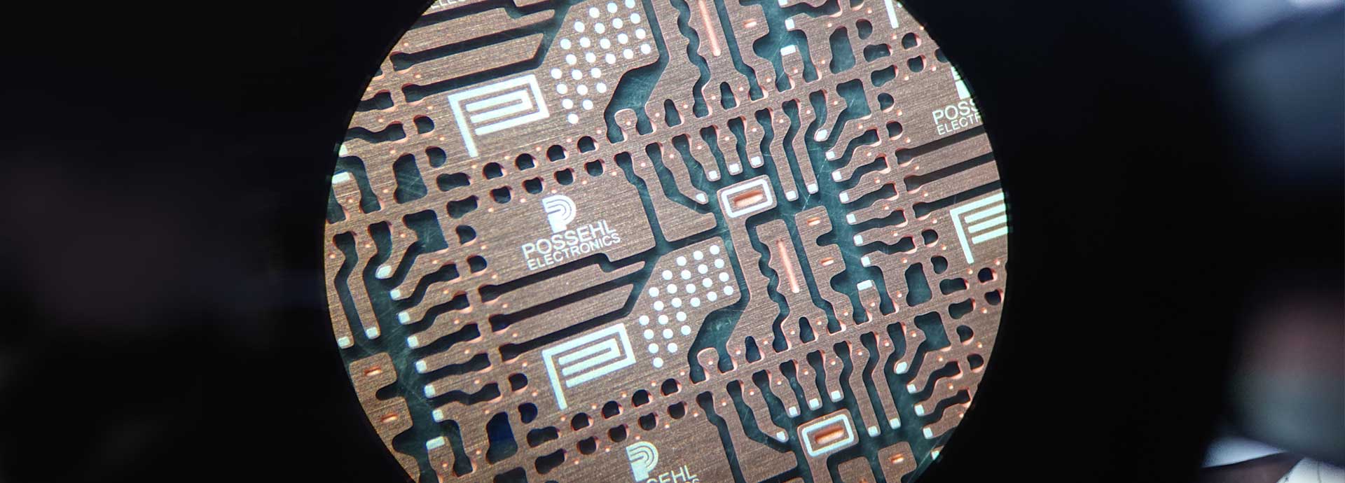
- By using the photo-mask technology we are able to achieve a positioning accuracy of +/-0.025 mm as well as a point-to-point spacing of at least 0.10 mm, both for Ag and for NiPdAu, on one or both sides.
- To improve the adhesion, we can roughen the copper surface on one or both sides prior to the coating process.
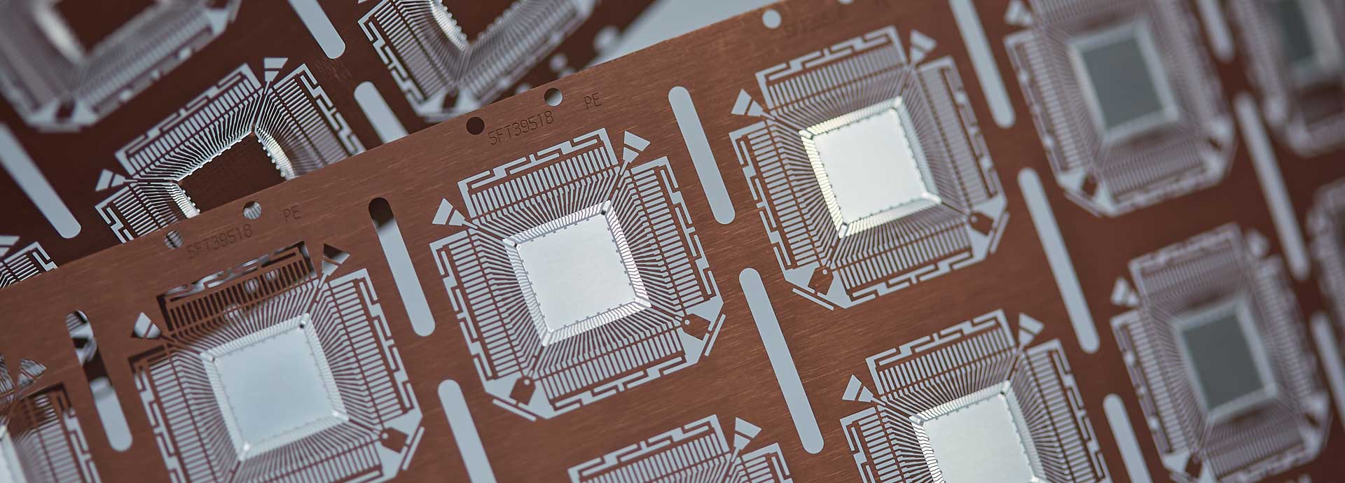
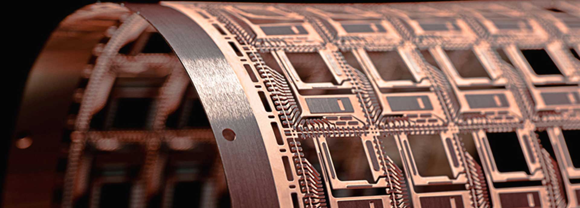
Etching
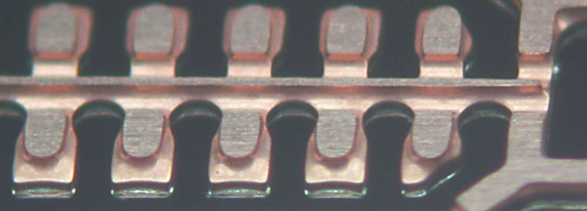
- We have the know-how to process highly complex designs with features such as cavity depth, deep etching, wettable flanks (dimples) and much more besides.
Treatment
- To improve the enclosure reliability (MSL-Level), we apply a proprietary treatment method to one or both sides of the copper surface to increase the mechanical locking performance.
Tools
- In-house production of printing templates and glass masks.
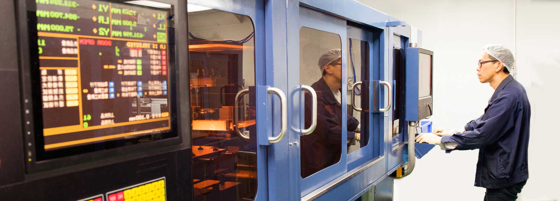
Machinery/Equipment
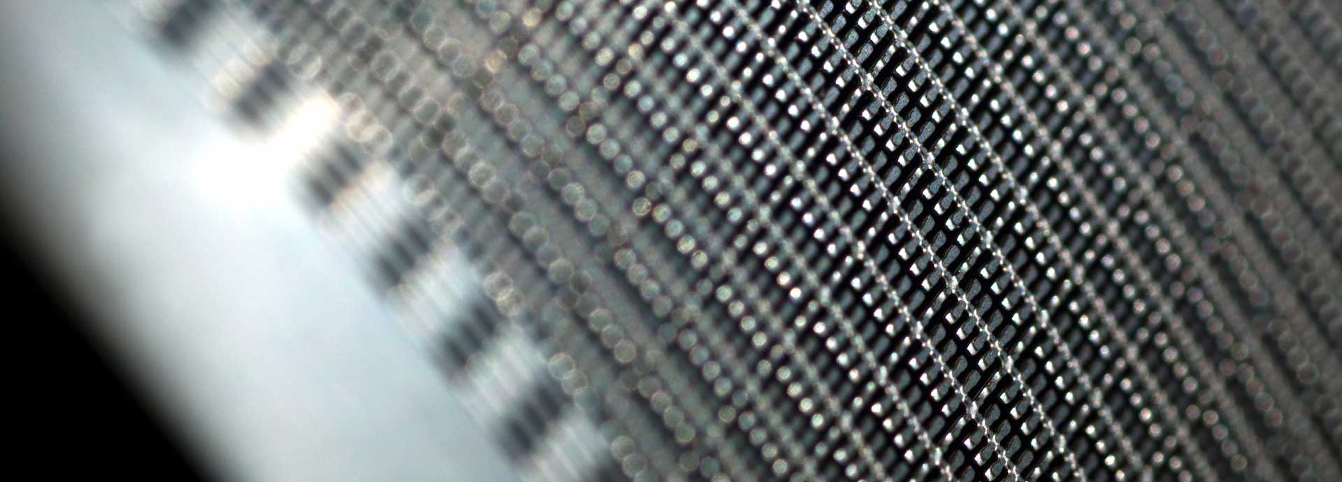
- High-speed reel-to-reel chemical etching process
- High-precision exposure process for design imaging
- Precise backside-strip-taping, lead/DAP offset, strip cutting
- Auto vision inspection systems are used in our process
Lead frame enclosure offer
- Enhance Cavity QFN-Design for a thinner enclosure
- Flipchip-QFN design with thin/long lines
- Deep half etching (on dambar) for 20mil QFN
- Selective coating both for an Ag and NiPdAu finish
- Etching ID marking on the pad
- Extension of the strip size up to 100×290 mm
- One-panel-wide lead frame design
- Super High Density design (>14,000 units per strip)
- Routable QFN lead frame design with 0.102 mm (4 mil) and 0.127 mm (5 mil) copper alloy thickness
- Fine Inner Lead Pitch up to 0.081 mm at a copper alloy thickness of 0.102 mm (4 mil)
- Multi-Pad Long Lead design QFN (under development)